
Building advanced quantum devices often means creating components at the atomic scale, like carefully placing individual light sources where they are needed. Achieving such precision is difficult, and then finding those precise components after they are made can be even harder, especially if it requires specialized equipment like super-cooled chambers. These challenges have long slowed the path to more practical quantum technologies.
However, a new approach described in a preprint appearing on arXiv by S. Eserin and colleagues offers a more efficient way to both create and quickly identify these crucial individual light sources, known as single emitters. Their work targets a specific type of silicon carbide crystal, called 4H-SiC, a material that shows great promise for future quantum computing and sensing.
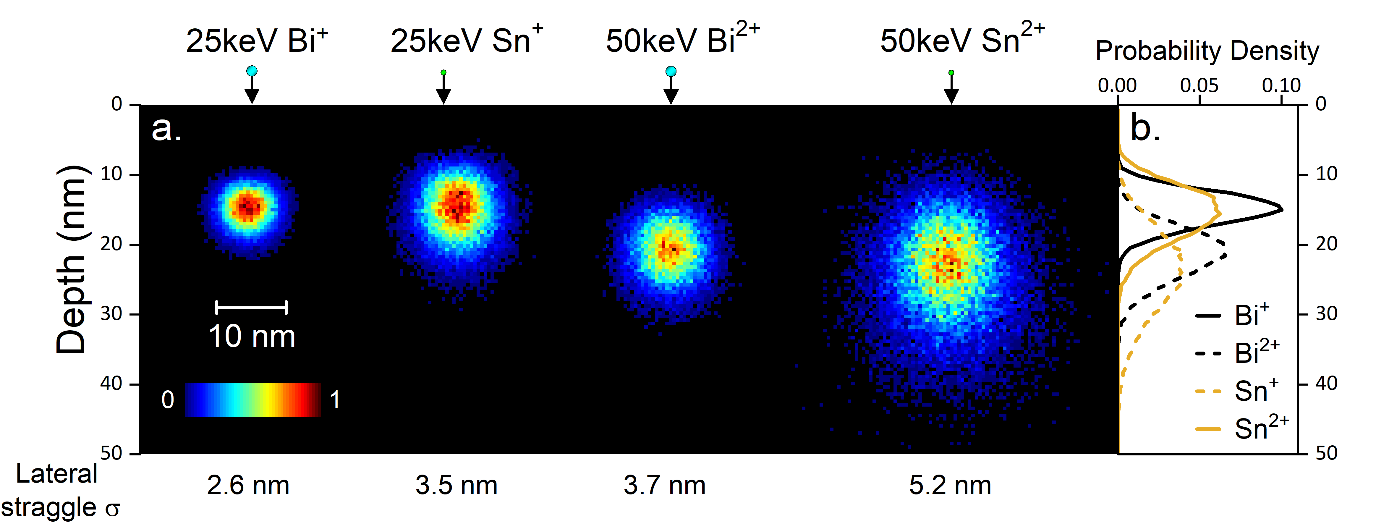
The process begins with crafting the single emitters themselves. Historically, implanting ions to create these light sources has been a known technique, with early examples dating back more than a decade in materials like diamond. The advance here is adapting this method for silicon carbide with a technique called maskless heavy ion implantation. This means researchers introduce atoms like bismuth and tin into the silicon carbide without needing intricate stencils, simplifying the manufacturing steps significantly. After this precise bombardment, the material undergoes a high-temperature bake, or annealing, at around 900 to 1000 degrees Celsius. This heating step is crucial; it helps repair any damage from the ion impacts and activates the desired light-emitting properties. This fabrication step yields specific practical results. After annealing, up to 18% of the implanted sites successfully host a single emitter. To put that in perspective, if you targeted 100 specific locations on the material, about 18 of them would become these useful, individual light sources. That is not every single spot, but it represents a notable success rate for a process requiring such atomic-level control, pushing past previous difficulties in scalable formation.
Once these single emitters are created, the next hurdle is finding and confirming them quickly. Traditional methods often rely on instruments that operate only at extremely cold temperatures, adding significant time and complexity to the process. This is where the second key innovation from S. Eserin and colleagues comes in: a tiered characterization scheme designed for rapid identification.
This scheme works like a multi-stage filter. First, the researchers quickly scan the material for bright spots, which act as preliminary candidates for single emitters. Next, they perform photon correlation measurements on these bright spots. This technique verifies if the light is indeed coming from a single source, rather than a cluster of sources or background noise. Finally, to definitively categorize the type of single emitter, they analyze its unique light characteristics, such as how its light is polarized, its maximum brightness, and its response to magnetic fields.
The most significant aspect of this identification method is that it can all be done at room temperature. This bypasses the need for the time-consuming low-temperature spectroscopy often required to differentiate between emitter types in other systems. Removing this bottleneck drastically speeds up the entire characterization process, making the development of quantum devices much more practical and efficient.
Why does this matter for quantum technologies? Single emitters are like the individual pixels or bits of information in future quantum devices. Their ability to reliably emit single particles of light, or photons, makes them essential for advanced quantum sensing, secure communication, and potentially quantum computing. The previous challenges of both creating these tiny, precise structures efficiently and then rapidly confirming their properties at room temperature have been major barriers to scaling up quantum technologies.
This work directly addresses those limitations. By providing an efficient maskless formation method and combining it with a streamlined, room-temperature identification scheme, Eserin and his team offer a clearer path towards deploying quantum technologies beyond specialized labs. While this research is still a preprint, awaiting full peer review, the methodical approach to both fabrication and characterization marks a careful step forward. It moves us closer to a future where individual light sources, precisely placed and quickly found, help power the next generation of quantum tools. ◆
Sourced from: "Efficient formation and identification of single emitters in 4H-SiC following maskless heavy ion implantation" by S. Eserin et al.